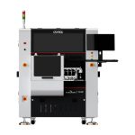
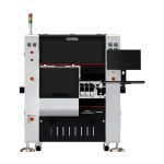
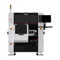
High-Accuracy Die Bonder
A die bonder is a high-precision semiconductor packaging machine used to pick and place bare semiconductor dies onto substrates, lead frames, or wafers with micron or sub-micron accuracy. It is a critical system in the back-end semiconductor assembly process, responsible for die attach, alignment, and bonding using epoxy, eutectic, or flip-chip interconnection technologies.
The Coreal High Accuracy Die Bonder is engineered for automated semiconductor assembly processes that require a balance of placement accuracy, production speed and material flexibility. It achieves a specified die attach accuracy of ±8 μm and supports dies ranging from 1 × 1 mm to 18 × 18 mm.
With a cycle time of 1.2 seconds per placement cycle, the machine is suitable for efficient semiconductor packaging and power module production. Actual production throughput depends on the die size, feeding method, vision inspection requirements, travel distance and selected bonding process.
The system can handle the mixed placement of semiconductor dies, solder preforms and electronic components, helping manufacturers reduce equipment transitions and consolidate multiple placement operations within one automated platform.
Bonding EquipmentTechnical Specifications
Equipment Dimensions
1430 × 1640 × 1750 mm
Equipment Weight
1800 kg
Die Size
1 × 1 mm to 18 × 18 mm
Die Attach Accuracy
±8μm
Cycle Time
1.2 S/C
Key Features of High Accuracy Die Bonder
● Micron-level placement accuracy for advanced semiconductor packaging
● High-speed pick-and-place system with stable throughput
● Advanced vision alignment system for real-time die positioning
● Compatible with epoxy, eutectic, and flip-chip bonding processes
● Precision force control to ensure consistent bonding quality
● Supports small chip, LED, MEMS, and IC packaging applications
● Fully automated or semi-automated production options available
Applications of Die Bonder Machine
High accuracy die bonding systems are widely used in modern microelectronics manufacturing, including:
● Semiconductor IC packaging and advanced chip assembly
● Flip-chip and 2.5D/3D IC integration
● LED chip and optoelectronic device manufacturing
● MEMS sensors and micro-devices
● RF modules and high-frequency devices
● Power electronics and automotive semiconductor packaging
Please visit our website for more information on this topic.