SWIR Cameras and Accessories in Semiconductor Inspection
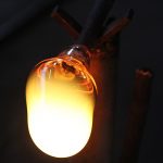
In the semiconductor inspection equipment, SWIR cameras can be used to inspect the quality of pure semiconductor material (usually silicon) after ingot growth. Furthermore, ingots that are subsequently sliced into wafers and these wafers can in a similar way be inspected for defects or cracks.
As the wafers are processed with successive layers to make transistors and memory cells used in modern integrated circuits, SWIR cameras are used to check alignment of the layers. High resolution scans of complete wafers are often accomplished with line scan cameras at the wafer defect inspection stage.
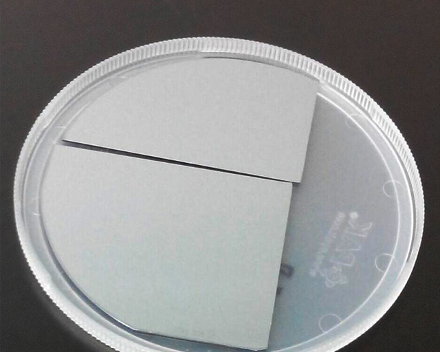
SWIR CAMERAS IMAGE OF SEMICONDUCTOR
RELATED PRODUCTS
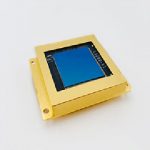
640 SWIR InGaAs High Cost-Performance Camera GigE
Zillion Techs SWIR camera is based on an in-house developed InGaAs detector with multiple resolutions.
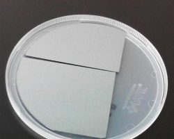
640 InGaAs VGA Area Sensor
GH-SW640 InGaAs area image sensors are two-dimensional image sensors.
MAG32 Online Thermal Imager
MAG32 is a high-quality thermal imager for all applications where superior image quality and measurement precision are both crucial.With an advanced high