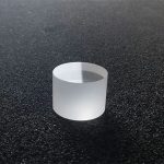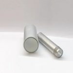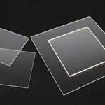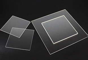
Wafers and Substrates
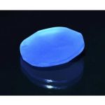
OST Photonics can supply lithium niobate (LiNbO3) wafers, lithium tantalate (LiTaO3) wafers, quartz single crystal wafers, various glass and fused silica wafers, GaAs wafers, SiC wafers, InP wafers, sapphire (Al2O3) wafers, Ge wafers and Si wafers in different specifications. Square plates, blanks and crystal boules are also available upon request. Other single crystal substrate materials including MgAl2O4, MgO, SrTiO3, LaAlO3, GGG, DyScO3, GdScO3, TbScO3, KTN, PMN-PT, LSAT, SrLaAlO4, YAG, YAlO3 (YAP) are also available on request.
What is the Difference Between SAW Grade Material and Optical Grade Material?
Optical grade materials are materials with low strain and no impurities, they are grown from the best raw materials at a relatively slow growth rate, and are often used in optical applications where the highest quality is required. Optical grade wafers are widely used in optical devices and require excellent optical performance.
SAW grade materials are primarily used in non-optical applications, and their growth raw materials rank second only to optical grade growth raw materials. The growth rate of this material is faster than that of optical grade material, which benefits mass production and cost-effectiveness.
In general, these grades of wafers vary in material quality and use. Optical grade wafers are considered to be of the highest quality, while SAW grade wafers are relatively lower in price. The selection of the appropriate wafer grade is crucial, depending on the specific application and material quality requirements.
FAQs of Wafers And Substrates
What is Epitaxy?
Epitaxial growth refers to the technique of growing crystalline layers with consistent crystal axes on a single crystal substrate, the epitaxial layer can be of the same material(Si/Si) or of different materials(SiGe/Si or SiC/Si).
What is the Pyroelectric Free Black LiNbO3/LiTaO3 Wafers?
We use a reduction technique to produce pyroelectric-free black LiNbO3/LiTaO3 wafers, which have a high ability to neutralize charges even if the electric potential occurs instantaneously. The pyroelectric effect of black LiNbO3/LiTaO3 wafers is almost eliminated and the transmittance is significantly reduced. The piezoelectric properties of black lithium niobate wafers are no different from those of standard wafers. Therefore, black-reduced lithium niobate wafers are widely used to produce higher-frequency surface acoustic wave devices.
What is the Difference Between Fused Silica and Quartz Single Crystal?
The key difference between fused silica and quartz single crystal is that fused silica contains non-crystalline silica glass whereas quartz contains crystalline silica. Fused silica is also known as fused quartz, it is a glass containing almost pure silica in an amorphous form. Quartz is a mineral compound containing silicon and oxygen atoms.
What is Single Crystal Substrate?
Single crystal substrate refers to the substrate materials used for epitaxial growth and the production of semiconductor devices.
What are Silicon Wafers Made?
Firstly, the silicon ore is purified to prepare polysilicon, and then the polysilicon is mixed with the dopant and melted for recrystallization to prepare a single crystal ingot. Finally, after ingot slicing, beveling, lapping, donor killing, polishing, cleaning, and other operations are performed to prepare silicon wafers with high flatness and surface cleanliness.
What is the Application of Silicon Wafer?
Silicon wafers are mainly used in various semiconductor chips, and then used in various electronic devices in daily life through various assembly, such as: TVs, computers, mobile phones, cars, etc.
What are the Advantages of Silicon as a Semiconductor Material?
1. The reserves of silicon on the earth reach 26.8%, second only to oxygen;
2. The energy gap of silicon is large (1.13V), which makes it have a higher operating temperature and lower leakage current;
3. The SiO2 layer on the surface of the silicon wafer can withstand high temperature and protect the silicon wafer.
What is the Relationship Between the Conductivity Type of the Silicon Wafer and the Dopant?
The dopants are mainly boron (B), phosphorus (P), arsenic (As), and antimony (Sb). Among them, the B-doped silicon wafer is P-type, which primarily conducts holes. The P-, As-, and Sb-doped silicon wafers are N-type and conduct electricity using electrons.