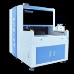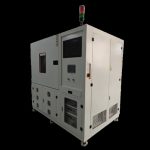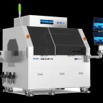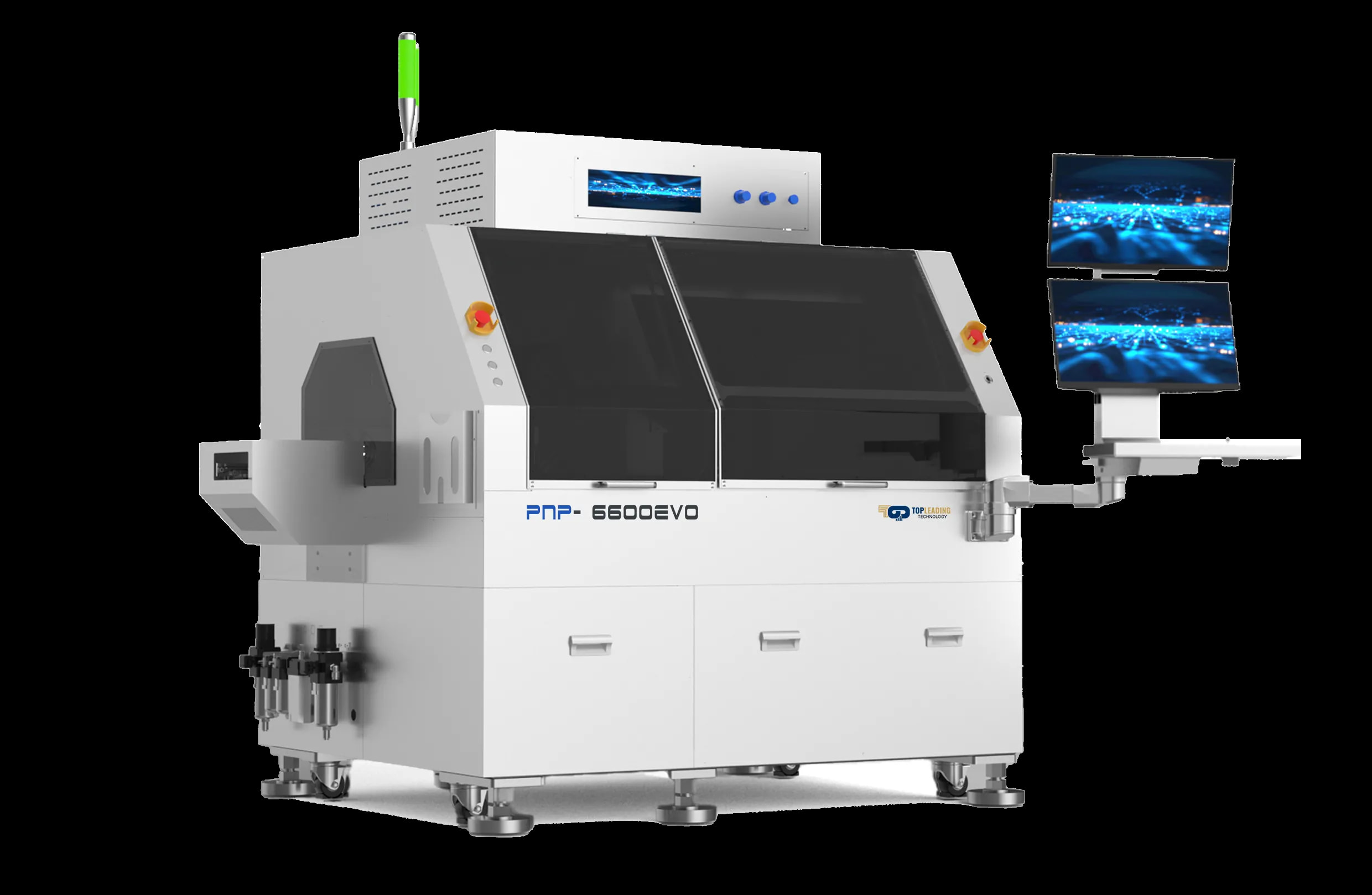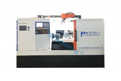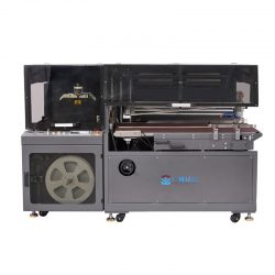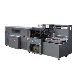
Die Bonder
Mainly used in the semiconductor packaging industry, it can be used for various types of integrated packaging.
Die Bonding Manufacturer – Top-leading
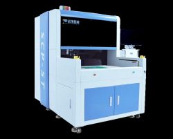
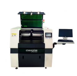
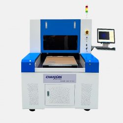
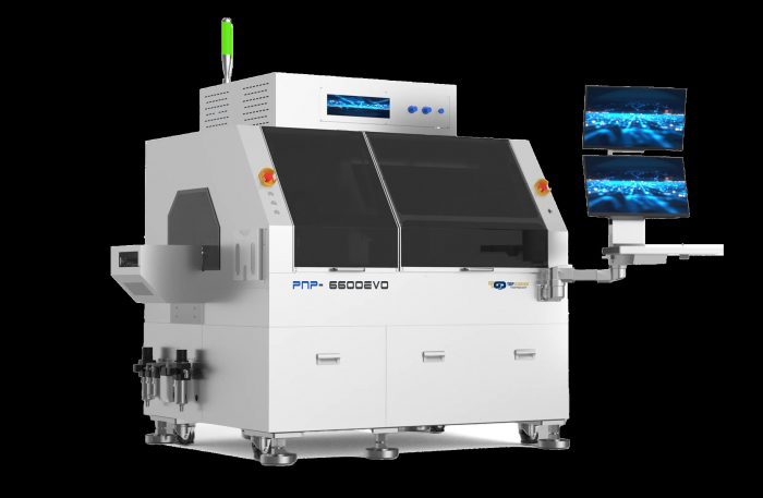
In back-end semiconductor manufacturing, the die attach process is a critical step. Top-leading’s die attach equipment is based on unique and innovative concepts, offering economic benefits to customers. The Top-leading Die Bonder is a high-precision assembly system engineered for fully automated die attachment in large-scale production environments. Its modular architecture ensures outstanding process reliability, high throughput, and exceptional flexibility.
What is a die bonder? The semiconductor chip manufacturing process is divided into two phases: front-end and back-end. The front-end processing phase involves projecting a circuit pattern onto the surface of a semiconductor wafer so that it is printed onto the wafer, while the back-end processing phase involves dicing the printed wafer into individual chips and assembling them into completed semiconductor devices.
Automatic Die Bonder
Top-leading’s automatic die bonder platforms deliver high-precision solutions for semiconductor and microelectronic assembly. Engineered for superior accuracy, unmatched flexibility, and rapid setup, these systems are ideal for a wide range of applications — from research and development and prototyping to high-mix and volume production.
Our die bonders support a broad variety of bonding techniques and component types, making them an excellent choice for advanced packaging and high-precision die attach processes, including:
· Hi-Rel Devices: High-reliability assemblies for aerospace and industrial applications.
· Medical Devices: Precision bonding for embedded or monitoring systems.
· Semiconductor Packaging: Attaching IC dies to packages or substrates.
· Optoelectronics: Assembly of laser diodes, LEDs, and optical modules.
· MEMS & Sensors: Integration of microelectromechanical systems and sensor chips.
· Power Electronics: Bonding high-power dies for automotive and industrial devices.
· RF & Microwave Modules: Assembly of high-frequency components.
Combining micron-level placement accuracy with high-speed operation and exceptional process flexibility, the equipment delivers both precision and performance. Standard features include multi-axis motion control (X, Y, Z, and Theta), vision alignment, and programmable bonding parameters. These capabilities ensure consistent and repeatable results across a wide range of die sizes and materials.
About us: https://www.topleadingintel.com/aboutus/